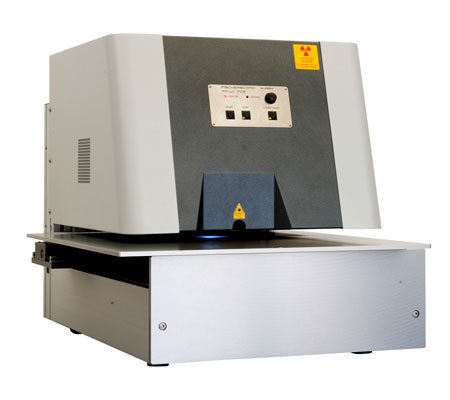
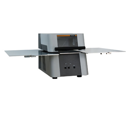
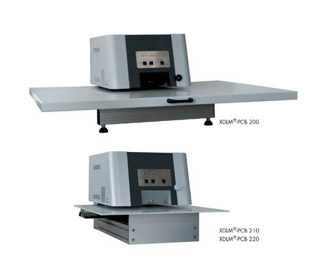
Send EMAIL

Logo

Application

PCB Coating Thickness Measurement Gauge : XDV-Micro PCB

Coating thickness measurement gauge for connectors XULM is available in various technical specifications. These are robust entry-level X-ray fluorescence measuring instruments for non-destructive material analysis and coating thickness measurement. Compact sized these devices are extensively acclaimed for their consistent performance, outstanding accuracy and longer service life. These are widely used for the non-destructive coating thickness measurement and material analysis.

ask for price
PCB Coating Thickness Measurement Gauge : XDV-μ PCB

Software Used : WinFTM®
Design Standards : DIN ISO 3497 and ASTM B 568

Typical fields of application

Measurements on very small flat components and structures on printed circuit boards in sizes up to 610 x 610 mm (24 x 24 in)

Analysis of very thin coatings, e.g., gold/palladium coatings of ≤ 0.1 μm (0.004 mils)

Automated measurements, e.g., in quality control

With 10 μm option: Measurements with smallest possible measurement spot in combination with a large silicon-drift-detector.

General Specification

Intended use:Energy dispersive x-ray fluorescence measuring instrument (EDXRF) to

measure thin coatings and multi-layer systems on printed circuit boards and

components.


Element range:Aluminum Al (13) to Uranium U (92) – up to 24 elements simultaneously.


Application:Optimal measurement conditions for applications with Au and Pd due to the

specific excitation characteristics of the polycapillary optics.

For further information contact your FISCHER representative.


Design:Bench-top unit with hood opening upwards and housing with a slot on

the side.

X/Y- and Z-axis electrically driven and programmable

Motor-driven changeable filters


Measuring direction:Top down


X-Ray Source/Detection

X-ray tube:Standard: Micro focus tube with tungsten target and beryllium window

Optional: Micro focus tube with molybdenum target and beryllium window


High voltage:Three steps: 10 kV, 30 kV, 50 kV


Primary filter:4x changeable: Ni 10 μm (0.4 mils); free; Al 1000 μm (40 mils);

Al 500 μm (20 mils)


X-ray opticsPolycapillary


X-Ray Source/Detection
Standard Non halo-free Option 20 μm Halo-free Option 10 μm Non halo-free
Measurement spot, fwhm at Mo-Kα appr. Ø 20 μm (0.8 mils) appr. Ø 20 μm (0.8 mils) appr. Ø 10 μm (0.4 mils)
X-ray detector Peltier-cooled silicon-drift-detector (SDD) Peltier-cooled silicon-drift-detector (SDD) Peltier-cooled silicon-drift-detector (SDD)
Effective detector area 20 mm2 (0.03 in2) 50 mm2 (0.08 in2) 50 mm2 (0.08 in2)


For halo-free capillaries, the radiation intensity for all energies of the x-radiation is concentrated on the nominal measurement spot. For capillaries,indicated as non halofree,radiation intensity with high energies (E > 20 keV) can cover a significantly larger area than the nominal measurement spot.


Sample Stage

Usable sample600 x 600 mm (23.6 x 23.6 in)

placement area

Width x depth:


Maximum travel:450 x 300 mm (17.7 x 11.8 in)


Max. travel speed XY:60 mm/s (2.4 in/s)


Repeatability precision XY:≤ 5 μm (0.2 mils), unidirectional


Max. sample weight:5 kg (11 lb)


Max. sample height:10 mm (0.4 in)


Sample Alignment

Video Microscope:High-resolution CCD color camera for optical monitoring of the

measurement location, manual focusing and auto-focus, with

contrast grid Crosshairs with a calibrated scale (ruler) and spot-

indicator,Adjustable LED illumination Laser pointer (class 1) to

support accurate specimen placement.


Zoom factor:Digital: 1x, 2x, 3x, 4x


Evaluation Unit

Computer:Windows®-PC


Software:Standard: Fischer WinFTM® LIGHT

Optional: Fischer WinFTM® BASIC, PDM®, SUPER


Electrical Data

Power supply:AC 115 V or AC 230 V 50 / 60 Hz


Power consumption:max. 120 W


Protection class:IP40


Dimensions

External dimensions:Width x depth x height [mm]: 670 x 885 x 660 mm (26.4 x 34.8 x25.9 in)


Weight:Approx. 156 kg (344 lb)


Environmental Conditions

Operating temperature:10 °C – 40 °C / 50 °F – 104 °F


Storage/Transport0 °C – 50 °C / 32 °F – 122 °F

temperature:


Admissible air humidity:≤ 95 %, non-condensing


Standards

CE approval:EN 61010


X-Ray standards:DIN ISO 3497 and ASTM B 568


Approval:Individual acceptance inspection as a fully protected instrument according

to the German regulations „Deutsche Röntgenverordnung-RöV“.


Get An Instant Quote

PCB Coating Thickness Measurement Gauge : XULM PCB

PCB coating thickness measurement gauge - XULM PCB is engineered under the firm direction of experts. These are specific X-Ray fluorescence measuring instrument widely used for measurements and analyses of coating thicknesses and compositions on printed circuit boards. These are specific robust entry-level instrument, widely recommended by large numbers of clients.

ask for price
PCB Coating Thickness Measurement Gauge : XULM PCB
Typical fields of application

Measurements on small components and structures on printed circuit boards in sizes up to 610 x 610 mm (24 x 24 in)

Measurements of functional coatings in the electronics and semiconductor industries

Determining of the composition of electroplating baths

General Specification

Intended use: Energy dispersive X-ray fluorescence measuring instrument (EDXRF)

to determine thin coatings and alloys.


Element range: Chlorine (17) to Uranium U (92) – up to 24 elements simultaneously.


Design: Bench-top unit with housing with a slot on the side

Fixed sample support


Measuring direction: Bottom up


X-Ray Source

X-ray tube: Micro focus tungsten tube with beryllium window


High voltage: Three steps 10 kV, 30 kV, 50 kV


Aperture (Collimator): Ø 0.1 mm (optional Ø 0.2 mm, slot 0.3 mm x 0.05 mm)


Measurement spot: Depending on the measuring distance and on the aperture, the actual

measurement spot size is shown in the video image. Smallest measurement

approx. Ø 0.2 mm


X-Ray Detection

X-ray detector: Proportional counter tube


Absorber: Optional cobalt or nickel absorber


Measurement distance: 0 … 27,5 mm (0 … 1.1 in) Distance compensation with patented DCM method

for simplified measurements at varying distances. For particular applications

or for higher demands on accuracy an additional calibration might be

necessary.


Sample Alignment

Video microscope:High-resolution CCD color camera for optical monitoring of the

measurement location along the primary beam axis, manual

focusing crosshairs with a calibrated scale (ruler) and spot-

indicator,adjustable LED illumination.


Zoom factor: Digital 1x, 2x, 3x, 4x


Sample Stage

Usable sample Without extension : 800 x 630 mm (31.5 x 24.8 in)

placement area: Without extension : 800 x 630 mm (31.5 x 24.8 in)

Width x depth: With extension : 1200 x 630 mm (47.2 x 24.8 in)


Max. sample size: 610 x 610 mm (24 x 24 in) with extension

Width x depth:


Max. sample weight: 5 kg (11 lb)


Max. sample height: 90 mm (3.5 in)


Electrical Data

Power supply: AC 115 V or AC 230 V 50 / 60 Hz


Power consumption: Max. 120 W


Protection class: IP40


Dimensions

External dimensions: Without extension : 800 x 800 x 560 mm (31.5 x 31.5 x 22 in)

Width x depth x height: With extension : 1200 x 800 x 560 mm (47.2 x 31.5 x 22 in)


Weight: Approx. 86 kg (190 lb)


Environmental Conditions

Temperature: Operation 10 °C – 40 °C / 50 °F – 104 °F


Temperature 0 °C – 50 °C / 32 °F – 122 °F

Storage/Transport:


Admissible air humidity: ≤ 95 %, non-condensing


Evaluation Unit

Computer: Windows®-PC


Software: Standard: Fischer WinFTM® BASIC including PDM®,

Optional: Fischer WinFTM® SUPER


Standards

CE approval: EN 61010


X-Ray standards:DIN ISO 3497 and ASTM B 568


Approval: Fully protected instrument with type approval according to the German

regulations "Deutsche Röntgenverordnung-RöV".


Get An Instant Quote

PCB Coating Thickness Measurement Gauge : XDLM PCB 210

Coating thickness measurement for PCB using XDLM PCB 210 is a qualitative range of devices available in various technical specifications. These are extensively acknowledged as specific X-ray fluorescence measuring instruments for measurements and analyses of coating thicknesses and compositions on printed circuit boards. These are acclaimed for its longer service life and outstanding accuracy.

ask for price
PCB Coating Thickness Measurement Gauge : XDLM PCB 210

Software Used : WinFTM®
Design Standards : DIN ISO 3497 and ASTM B 568

Typical fields of application

Measurements on small components and structures on printed circuit boards in sizes up to 610 x 610 mm (24 x 24 in)

Measurements of functional coatings in the electronics and semiconductor industries

XDLM-PCB 210 and 220: Automated measurements, e.g., in quality control

Determining the composition of electroplating baths

General Specification

Intended use:Energy dispersive x-ray fluorescence measuring instrument (EDXRF)

to determine thin coatings, small structures and alloys.


Element range:Chlorine (17) to Uranium U (92) – up to 24 elements simultaneously.


Design:Bench-top unit with housing with a slot on the side


Measuring direction:Top down


X-Ray Source

X-ray tube:


High voltage:Three steps: 30 kV, 40 kV, 50 kV


Aperture (Collimator):XDLM-PCB 200/210: Ø 0.1 mm (3.9 mils), optional Ø 0.2 mm (7.9 mils),

slot 0.3 x 0.05 mm (11.8 x 2 mils)


Standard (523-440): Ø 0.1 mm (3.9 mils); Ø 0.2 mm (7.9 mils); 0.05 x 0,05 mm

(2 x 2 mils); 0.2 x 0.03 mm (7.9 x 1.2 mils)


Optional (523-366): Ø 0.1 mm (3.9 mils); Ø 0.2 mm (7.9 mils); Ø 0.3 mm (11.8

mils); 0.3 x 0.05 mm (11.8 x 2 mils)


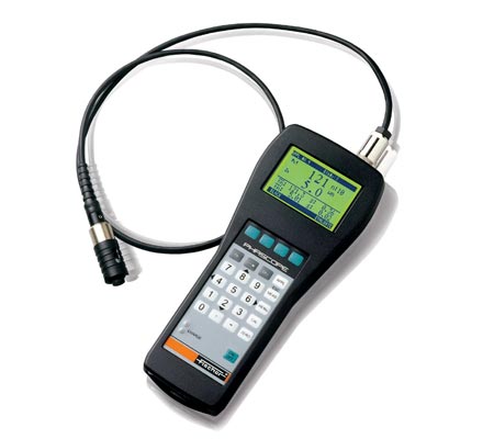
Measurement spot:Depending on the measuring distance and on the aperture, the actual

measurement.Spot size is shown in the video image.

Smallest measurement spot:approx. Ø 0.2 mm (7.9 mils)


Measurement distance:0 … 10 mm (0 … 0.4 in) Distance compensation with patented DCM for

simplified measurements at varying distances.For particular applications

or for higher demands on accuracy an additional calibration might be

necessary.

X-Ray Detection

X-ray detector:Proportional counter tube


Sample Alignment

Sample positioning:Manually


Video microscope:High-resolution CCD color camera for optical monitoring of the

measurement location along the primary beam axis, Manual

focusing and auto-focus, Crosshairs with a calibrated scale

(ruler) and spot-indicator, Adjustable LED illumination,Laser

pointer (class 1) to support accurate,specimen placement.


Zoom factor:Digital 1x, 2x, 3x, 4x


Evaluation Unit

Computer:Windows®-PC


Software:Standard: Fischer WinFTM® LIGHT

Optional: Fischer WinFTM® BASIC, PDM®, SUPER


Dimensions

Dimensions
XDLM-PCB 200 XDLM-PCB 210
External dimensions 610 x 750 x 450 mm With maximum XY travel range:
1000 x 1265 x 470 mm
(39.4 x 49.8 x 18.5 in)
Width x depth x height With extension:
1200 x 1050 x 450 mm
(47.2 x 41.3 x 17.7 in)
XY table retracted in home position:
650 x 810 x 470 mm
(25.6 x 31.9 x 18.5 in)
Weight Approx. 86 kg (190 lb) Approx. 86 kg (190 lb)

Sample support stage

Sample Stage
XDLM-PCB 200 XDLM-PCB 210/220
Design Fixed sample support with manual pop out function Programmable XY-stage with pop out function
Usable sample placement area 600 x 600 mm (23.6 x 23.6 in)
With extension:
1200 x 900 mm (47.2 x 35.4 in)
600 x 600 mm (23.6 x 23.6 in)
Maximum travel XY-axis - 450 x 300 mm (17.7 x 11.8 in)
Max. travel speed XY - 450 x 300 mm (17.7 x 11.8 in)
60 mm/s (2.4 in/s)
Repeatability precision XY - ≤ 0.01 mm (0.4 mils), unidirectional
Max. sample Weight 5 kg (11 lb) 5 kg (11 lb)
Max. sample Height 5 mm 5 mm

Electrical Data

Power supply:AC 115 V or AC 230 V 50 / 60 Hz


Power consumption:max. 120 W


Protection class:IP40


Environmental Conditions

Operating temperature:10 °C – 40 °C / 50 °F – 104 °F


Storage/Transport0 °C – 50 °C / 32 °F – 122 °F

temperature:


Admissible air humidity:≤ 95 %, non-condensing


Standards

CE approval:EN 61010


X-Ray standards:DIN ISO 3497 and ASTM B 568


Approval:Fully protected instrument with type approval according to

theGerman regulations "Deutsche Röntgenverordnung-RöV".


Get An Instant Quote

PCB Coating Thickness Measurement : PHASCOPE® PMP10

“Hand-held instrument for measuring coating thickness on PC Boards and electroplated surfaces. The hand-held PHASCOPE® PMP10 is ideally suited for quality control in the electroplating and printed circuit board (PCB) industries. Because the instrument employs the phase-sensitive eddy current method (ISO 21 968), it allows the measurement of metal coatings on any substrate. A specially designed probe even enables measurements in PCB throughholes.”

ask for price
PCB Coating Thickness Measurement Phasoscope : PMP 10
Typical areas of application are:

Measuring copper thickness in PCB through-holes, especially on thick PC Boards.

Measuring coating thickness of nickel on steel

Measuring zinc or copper on steel – despite rough surfaces and complex surface geometries

Measuring the thickness of non-ferrous metals on non-ferrous metals, given sufficient difference in conductivity, e.g. copper on brass or bronze

Measuring the thickness of non-ferrous metals on insulating substrates, such as copper layers on circuit boards.

Sheet metal processing

Paint/zinc on iron, e.g. thin EPD coatings

Paint on aluminium

Paint on steel

Brake line tubing

Wire (mesh and lattice), e.g. shopping trolleys

The PHASCOPE® PMP10 DUPLEX combines three measurement methods

Magnetic induction method For measuring the overall thickness of paint and

Amplitude-sensitive eddyFor measuring a single paint layer on aluminium

current method DIN EN

ISO 2360:


Phase-sensitive eddyFor measuring zinc coatings on iron,

current method ISOirrespective of overlying paint layers

21968:


Instrument features

DUPLEX measuring mode: display of paint on zinc on iron or paint on aluminium

DUAL measuring mode: display of total thickness (paint and zinc) on iron or paint on aluminium

Extensive evaluation and statistics functions

Outlier control and tolerance monitoring options

Various languages to choose from

Battery and/or continuous operation via plug-in charger (included)

Storage of up to 20,000 readings

Data transfer via RS232 interface

Get An Instant Quote

PCB Coating Thickness Measurement : Couloscope CMS

The CMS2 measures the thickness of virtually any metallic coating, including multi-layer, on any substrate material; it works according to the coulometric method by anodic dissolution (DIN EN ISO 2177). The simple handling and menu-supported operator guidance makes the CMS2 the ideal solution for both production monitoring in the electroplating industry and incoming inspection on finished parts.

The device comes equipped with nearly 100 predefined measuring applications for different coating systems (e.g. zinc on iron, nickel on brass), as well as various de-plating speeds (e.g. 1, 2, 5, and 10 μm/min). These can also be combined for measuring multi-layer systems.
The robust and user-friendly Couloscope CMS2 is suitable for both production monitoring in the electroplating industry and incoming inspection on finished parts.

ask for price
PCB Coating Thickness Measurement : Couloscope CMS
Features

Large, high-resolution colour display

Simple instrument operation and graphically supported user guidance

Partially-automated measurement with support stand V18 Simple selection of de-plating speed (0.1 – 50 μm/min) and de-plating area (0.6 – 3.2 mm Ø)

Graphic display of the voltage profile in the measuring cell

Graphic and statistical analysis options

Various languages and measurement units to choose from

Typicial Field Of Application

Electroplated fasteners

Testing the remaining pure tin content on printed circuit boards

Chrome plated bathroom fittings

Common single and duplex coatings, such as ZN on iron or SN/NI on copper, can be measured

Accurate measurements of metal coating in the thickness range of 0.05 - 50 μm, no pre-settings are required for many materials; substrate composition and geometry are also irrelevant to the measuring process

Measurement of the remaining pure tin on printed circuit boards in order to ensure solderability

Multi-layer coatings such as CR/NI/CU on iron or plastic (abs) substrates

Get An Instant Quote

Looking for Product Name ?

x

Send SMS Enquiry

*Please Enter Requirment

*Please Enter valid Mobile Number

*Please Enter Proper Name